Rough automatic draft, low quality: expect mistakes and awkward wording. It will be replaced by a better translation. Original →
8
Conductors, semiconductors and dielectrics
Before talking about the semiconductor diode and transistor, we will talk about what semiconductors are, what their internal structure is and what properties they have.
Of the large number of semiconductors known in nature, silicon and germanium are the most studied. These are elements numbered 14 and 32 in the periodic table.
Strictly speaking, semiconductors are dielectrics, only very weak dielectrics. Weak in the sense that they are easy to convert into semiconductors. There are several ways to do this. The main ones are: irradiation, bombardment of semiconductors with fast particles, heating and adding appropriate impurities to the semiconductor.
As you know, dielectrics do not conduct electric current, that is, they are insulators. If a potential difference is created at the ends of a dielectric sample and the current is changed, it will be equal to zero. This is explained by the fact that inside the sample there are no free loaded particles, for example, electrons, which, under the influence of an electric field, would move from one end of the sample to the other and thus create a current. The dielectric atoms firmly hold all their electrons and even if they release them from themselves, they have only exchanged with their neighbor for another electron.
It’s a different matter in metal. The bulk of electrons there behave similarly to electrons in a dielectric. But some of them, those that are located far from the positively charged nuclei and are therefore weakly connected with them, during the formation of a crystal receive such freedom that they can be throughout the entire crystal. These electrons are called free electrons, or conduction electrons. If you place a metal in an electric field, then these
9
free electrons (because they have a negative charge) move in the direction opposite to the direction of the electric field. The electric field, like wind, blows them towards the boundary of the sample. A galvanometer connected in this way will register an electric current.
So, a dielectric does not conduct electric current because there are no free charge carriers in it that can move freely along the sample under the influence of an electric field.
But we ourselves can create such charges. One of the ways is to act on the atom of the dielectric with some suitable “tool”, for example, a quantum of light - a photon. We irradiate the dielectric with ordinary light, or even better, RENTen rays, since they have higher energy, and knock out electrons from the atoms that form the crystal. In this way, free electrons can be created in the dielectric and turned into a conductor. It is clear that the energy required to release an electron depends primarily on what atoms the crystal is made of and how these atoms are located in the crystal. In other words, this energy is different for different crystals. The minimum energy required to remove an electron from an atom and convert it into a free one is called the energy gap of a given dielectric. If radiation falls on the crystal, the energy of the quanta of which is lower than the minimum energy required to release an electron, then none of the electrons will be knocked out and the dielectric will remain an insulator.
The difference between dielectrics and semiconductors lies precisely in the size of the energy gap. Dielectrics with a sufficiently small energy gap are called semiconductors. The energy gap of semiconductors is approximately 10 times smaller than that of pronounced dielectrics, such as, for example, diamond. The energy gap width for diamond is 7 38, while for thermanium we have 0.72 38, and for silicon 1.1 38*). Thus, in order to turn a semiconductor into a conductor, it is enough to impart it to electrons relatively small small small small small smallest.
Now imagine that we are heating a dielectric. As the temperature increases, the average energy of the electrons will increase, and many of them will have enough energy to bridge the energy gap. As a result, there are more and more free electrons, and the appearance of free electrons occurs more often the higher the temperature, and, of course, most often in those crystals that have a smaller energy gap, that is, in semiconductors. That is why semiconductors are called semiconductors, because at sufficiently high temperatures (for example, room temperature ~300°K) they are conductors, and when the temperature drops they turn into dielectrics. The transistor example transmits work in freezing cold, since the semiconductors used in its transistors turn into real insulators.
Electrons and holes
Let us somehow knock out an electron from a dielectric atom and it flies away from this atom. In the crystal, in this place, a non-chewing electron or, as they say, a hole is formed. The interesting thing is that the hole does not stand still, but begins to move and generally behaves like a positively charged particle. Here’s how it happens.
When some atom lacks an electron, the electron can transfer
*)1 electron-volt (1 38) - the energy acquired by an electron when passing through a potential difference of 1 volt. 1 38=1.6·10⁻¹⁹ j.
10
reck from a neighboring atom that has as many electrons as needed (Fig. 1, a). But then a shortage of electrons is detected on the neighboring atom, that is, the hole moves to the neighboring atom (Fig. 1, b). Of course, in reality it is electrons from filled atoms that jump to neighboring unfilled ones, but it is more convenient to talk about the movement of a hole. There is still only one hole, but it reflects the movement of many electrons. The movement of a hole is similar to the movement of a positively charged particle, because if, under the influence of an electric field, electrons move in one direction, then their “lack” moves in the other.
It will be useful to highlight the difference between the behavior of metals and semiconductors in an electric field. Current in a metal is created only by free electrons. Metal is structured in such a way that it always contains one or another amount of them. In a semiconductor, at sufficiently low temperatures, there are no free electrons. These free electrons
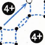
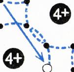
Fig. 1.
can be created. But at the same time, by tearing an electron away from the atom and presenting it with freedom, we also create a hole. Subsequently, these electrons and holes move independently of each other. It turns out that the current in a semiconductor consists of the electron current and the hole current.
It may happen that a free electron and a hole meet, that is, that an electron, while moving through a crystal, encounters an atom that just lacks an electron. It will occupy this free space, and at this moment both the electron and the hole will disappear. In this case, a recommendation is said to have occurred. You have the right to ask, why then create electrons and holes if sooner or later they will simply destroy each other? First, in the presence of an electric field, electrons and holes, as particles with different charges, move in opposite directions, and we can detect the current they create even before they recombine. Secondly, we do not knock out electrons from every atom, but, for example, from every thousandth. In this case, we create a significant current (since there are approximately atoms in each cubic centimeter of the crystal) and leave enough freedom for the movement of electrons and holes.
Semiconductor crystals are grown extremely pure. This is also done so that nothing interferes with the movement of electrons and holes.
Donors and Accelerators
There is also a way to create free electrons in a semiconductor. Let us imagine a thermanium crystal in which one of the thermanium atoms is replaced by an arsenic atom. Thermanium atoms have a valency of 4, and arsenic atoms have a valence of 5. When an arsenic atom is surrounded by thermanium atoms, the fifth
11
The electron of arsenic is bound to it very weakly (Fig. 2). To tear it off, an energy of 0.1 eV is sufficient, which does not exceed the thermal energy of the crystal. Thus, one of the electrons of arsenic atoms becomes free and flows through the crystal. By introducing impurities of higher valency into the semiconductor, we can always obtain a sufficient number of negative current carriers. In this case, the impurity atoms are called donors, and the semiconductors themselves containing donor-type impurities are called -type semiconductors.
It is possible to introduce trivalent atoms, for example, aluminum, into a thermanium crystal. An aluminum atom, in order to sit firmly in a thermanium crystal, must have two outer electrons, so it captures the missing electron from neighboring thermanium atoms (Fig. 3). A hole is formed in the crystal. Impurity atoms of this type are called acceptors, and semiconductors are called -type semiconductors.
- and -type semiconductors have a corresponding excess number of negative or positive current carriers. Beaten - in comparison with those electrons and holes that create thermal excitations. However, the overall mystery of semiconductors is, of course, zero, since their crystals are formed from neutral atoms. The negative supply of electrons in a -type semiconductor is compensated by positively charged donor centers fixed at the sites of the crystal lattice, for example, arsenic atoms. In a -type semiconductor, the positive riddle gives rise to twos of the negative riddle of the accelerator centers.
Transitions between semiconductors
Let’s take two different samples of termanium (- and -types) and apply them to each other ). We are interested in what will happen at the interface (Fig.4).
Until the contact between the samples was created, electrons in the -region and holes in the -region, approaching the sample boundary, were reflected from the surface and returned deep into the semiconductor. How
) From the root “accett” - to accept.
12
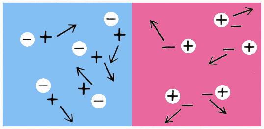
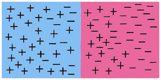
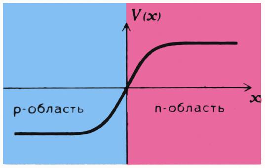
Fig. 4.
As soon as a transition is formed, the situation changes. Electrons from the region moving towards the interface have the opportunity to jump to the region. Similarly, holes from the -area will be counted into the -area. Both of these processes act in the same direction: they tend to charge the -type term positive, and the -type term negative. In fact, the -region, the total charge of which was equal to zero, now becomes positively charged, donating negatively charged electrons to the -region. Positively charged holes coming from the -region only contribute to this. Thermal -type acquires a negative charge both due to the arrival of electrons and the departure of holes.
However, all this process must be left behind or later. When the -type thermal is charged positively, and the -type thermal is charged negatively, then a capacitor is formed, and an electric field appears at the boundary, directed from the -region to the -region (Fig. 5). This means that, for example, electrons from the -region will no longer be able to go to the -region. A strong electric field at the boundary will cause them to turn back. The same can be said for holes. The resulting electric field will reduce their chances of moving into the -region. So, an equilibrium will occur in which the -type thermal will be positively charged, and the -type thermal will be positively charged.
Fig. 5.
negative, and at the boundary there will be a strong electric field directed from the -region to the -region.
If we take the potential of the electric field at the boundary to be zero, then the potential of the -region is greater than zero, and the potential of the -region is less than zero (Fig. 6), as will be the plate of a charged capacitor. The potential changes sharply in the region where the electric field exists, i.e., at the interface between - and -type thermals. The potential difference in the - transition is equal to the energy that an electron needs to have to move from the region to the region, or a hole to transition from the region to the region. As for holes in the -region and electrons in the -region, if they are lucky enough to accidentally get to the interface, the electric field will only push them into another region. However, if this happens, then this leads to a decrease in the charge of both the and regions, i.e., to a decrease in the transfer
13
a drop in potential at the boundary and a decrease in the electric field.
But then it will find electrons in the -region and holes in the -region, which have sufficient energy to overcome the diminished potential bartender ). They will flow through the barrier, and balance will be restored. We see that the equilibrium between the - and -regions is dynamic. There will always be an exchange of electrons and holes between them, but this exchange is equivalent: the average charge of the - and -regions remains unchanged and, therefore, the potential drop and the electric field at the boundary remain unchanged. However, the total current across the boundary is zero. This equilibrium can only be disrupted by creating an external potential difference at the ends of the — junction. Let us now consider this case.
Semiconductor diode
A sample with a — junction has one important property: it can work as a diode, that is, a system that passes current in only one direction.
Let’s see what happens if we turn on the — transition in the electrical target, that is, we create an external potential difference at the ends of the sample. There are two possible cases. Either the potential drop at the – transition boundary increases or decreases. the balance between the and regions, carried out through the exchange of electrons and holes, is disrupted, and the average current across the boundary remains depending on whether the outer direction of the potential increases or decreases, which exists in transition by itself.
If the external direction increases at the boundary, that is, reduce the potential difference if it increases, and vice versa. However, he fails to do this due to the transition to an electrical target. The average charge transferred from one side of the — junction to the other is not retained in the sample, but goes further along the chain. the balance remains disrupted.
So, when turning on the —-transition under the direction, the exchange of charge
14
between the - and -regions changes and current flows through the junction. This current is very large at one level of external voltage and very small at another.
The property of a semiconductor diode to pass current in only one direction is used, for example, to create rectifiers - devices that convert alternating current into direct current.
The simplest circuit of such a rectifier is shown in figure 7. To analyze the operation of this circuit, the only important thing for us is the fact that with one direction symbol the resistance of the diode () is practically equal to zero (when it passes a huge current), and with another direction symbol the diode practically does not conduct current and, therefore, its resistance is very high.
Now suppose that the diode allows current to pass only from left to right, that is, it is open when the input direction is greater than zero, and closed when it is negative.
At total circuit resistance
and the output direction will be practically equal to the input.
At the diode resistance is infinite (), and therefore the direction of is practically zero. the output direction is zero. Thus, our system converts an alternating direction into a constant direction.
Transistor
Now we can consider a transistor - a system that combines the two transitions just discussed. A -transistor is a small block made, for example, of thermium, composed of three sections: -region, -region and again -region (Fig. 8). Each transition in the transistor behaves as described above. In particular, in each transition there should be a potential drop - a drop from the -region to each of the -regions, so that the overall potential distribution will be as shown in figure 8.
In a working transistor, each of the three areas is connected to the source